- 您现在的位置:买卖IC网 > Sheet目录308 > ADUM5240ARZ-RL7 (Analog Devices Inc)IC ISOLATOR 2CH W/CONV 8-SOIC
�� �
�
�ADuM5240/ADuM5241/ADuM5242�
�Given� the� geometry� of� the� receiving� coil� in� the� ADuM524x� and�
�an� imposed� requirement� that� the� induced� voltage� be� at� most�
�50%� of� the� 0.5� V� margin� at� the� decoder,� a� maximum� allowable�
�magnetic� field� is� calculated,� as� shown� in� Figure� 13.�
�100�
�10�
�1�
�0.1�
�0.01�
�0.001�
�1k� 10k� 100k� 1M� 10M� 100M�
�MAGNETIC� FIELD� FREQUENCY� (Hz)�
�Figure� 13.� Maximum� Allowable� External� Magnetic� Flux� Density�
�For� example,� at� a� magnetic� field� frequency� of� 1� MHz,� the�
�maximum� allowable� magnetic� field� of� 0.2� kgauss� induces� a�
�voltage� of� 0.25� V� at� the� receiving� coil.� This� is� about� 50%� of� the�
�sensing� threshold� and� does� not� cause� a� faulty� output� transition.�
�Similarly,� if� such� an� event� were� to� occur� during� a� transmitted�
�pulse� (and� was� of� the� worst-case� polarity),� it� would� reduce� the�
�received� pulse� from� >1.0� V� to� 0.75� V—still� well� above� the� 0.5� V�
�sensing� threshold� of� the� decoder.�
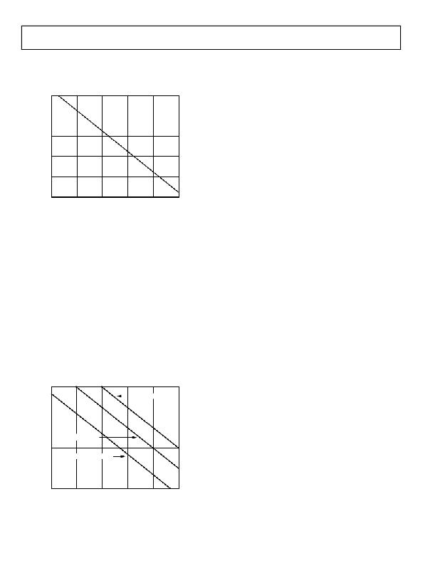
�The� preceding� magnetic� flux� density� values� correspond� to�
�specific� current� magnitudes� at� given� distances� from� the�
�ADuM524x� transformers.� Figure� 14� expresses� these� allowable�
�current� magnitudes� as� a� function� of� frequency� for� selected�
�distances.� As� shown� in� Figure� 14,� the� ADuM524x� is� extremely�
�immune� and� can� only� be� affected� by� extremely� large� currents�
�operated� at� high� frequencies� very� close� to� the� component.� For�
�the� 1� MHz� example� noted,� one� would� have� to� place� a� 0.5� kA�
�current� 5� mm� away� from� the� ADuM524x� to� affect� the� operation�
�of� the� component.�
�1000�
�DISTANCE� =� 1m�
�100�
�10�
�Data� Sheet�
�Note� that� at� combinations� of� strong� magnetic� field� and� high�
�frequency,� any� loops� formed� by� printed� circuit� board� (PCB)�
�traces� could� induce� error� voltages� sufficiently� large� enough� to�
�trigger� the� thresholds� of� succeeding� circuitry.� Care� should� be�
�taken� in� the� layout� of� such� traces� to� avoid� this� possibility.�
�THERMAL� ANALYSIS�
�Each� ADuM524x� component� consists� of� two� internal� die,�
�attached� to� a� split-paddle� lead� frame.� For� the� purposes� of�
�thermal� analysis,� it� is� treated� as� a� thermal� unit� with� the� highest�
�junction� temperature� reflected� in� the� θ� JA� value� in� Table� 2.� The�
�value� of� θ� JA� is� based� on� measurements� taken� with� the� part�
�mounted� on� a� JEDEC� standard� 4-layer� PCB� with� fine-width�
�traces� in� still� air.� Under� normal� operating� conditions,� the�
�ADuM524x� operates� at� full� load� across� the� full� temperature�
�range� without� derating� the� output� current.� For� example,� a� part�
�with� no� external� load� drawing� 80� mA� and� dissipating� 400� mW�
�causes� a� 32°C� temperature� rise� above� ambient.� It� is� normal� for�
�these� devices� to� run� warm.�
�Following� the� recommendations� in� the� PCB� Layout� section�
�decreases� the� thermal� resistance� to� the� PCB� allowing� increased�
�thermal� margin� at� high� ambient� temperatures.�
�PCB� LAYOUT�
�The� ADuM524x� requires� no� external� circuitry� for� its� logic�
�interfaces.� Power� supply� bypassing� is� required� at� the� input� and�
�output� supply� pins� (see� Figure� 15).�
�The� power� supply� section� of� the� ADuM524x� uses� a� 300� MHz�
�oscillator� frequency� to� pass� power� through� its� chip� scale� trans-�
�formers.� In� addition,� the� normal� operation� of� the� data� section�
�of� the� i� Coupler� introduces� switching� transients,� as� described� in�
�the� DC� Correctness� and� Magnetic� Field� Immunity� section,� on�
�the� power� supply� pins� (see� Figure� 11).� Low� inductance� capacitors�
�are� required� to� bypass� noise� generated� at� the� switching� frequency�
�as� well� as� 1� ns� pulses� generated� by� the� data� transfer� and� dc� refresh�
�circuitry.� The� total� lead� length� between� both� ends� of� the� capacitor�
�and� the� input� power� supply� pin� should� not� exceed� 20� mm.�
�In� cases� where� EMI� emission� is� a� concern,� series� inductance� may�
�be� added� to� critical� power� and� ground� traces.� Discrete� inductors�
�should� be� added� to� the� line� such� that� the� high� frequency� bypass�
�capacitors� are� between� the� inductor� and� the� ADuM524x� device�
�pin.� Inductance� can� be� added� in� the� form� of� discrete� inductors�
�or� ferrite� beads� added� to� both� power� and� ground� traces.� The�
�1�
�DISTANCE� =� 100mm�
�recommended� value� corresponds� to� impedance� between� 50� ?�
�and� 100� ?� at� approximately� 300� MHz.�
�0.1�
�DISTANCE� =� 5mm�
�If� the� switching� speed� of� the� data� outputs� is� causing� unacceptable�
�EMI,� capacitance� to� ground� can� be� added� at� output� pins� to� slow�
�the� rise� and� fall� time� of� the� output.� This� slew� rate� limits� the� output.�
�Capacitance� values� depend� on� application� speed� requirements.�
�0.01�
�1k�
�10k�
�100k�
�1M�
�10M�
�100M�
�See� the� AN-0971� Application� Note� for� board� layout� guidelines.�
�MAGNETIC� FIELD� FREQUENCY� (Hz)�
�Figure� 14.� Maximum� Allowable� Current�
�for� Various� Current-to-ADuM524x� Spacings�
�Rev.� B� |� Page� 12� of� 16�
�发布紧急采购,3分钟左右您将得到回复。
相关PDF资料
ADUM5400CRWZ-RL
IC ISOLATOR 4CH DCDC CONV 16SOIC
ADUM5402WCRWZ
IC ISOLATOR 4CH DCDC CONV 16SOIC
ADUM5404CRWZ
IC ISOLATOR 4CH DCDC CONV 16SOIC
ADUM6132ARWZ-RL
IC GATE DRIVER ISOLATED 16-SOIC
ADUM6201CRIZ
ISOLATED DC-DC CONV 2CH 16SOIC
ADUM6404ARWZ
IC ISOLATOR 4CH DCDC CONV 16SOIC
ADUM7241CRZ-RL7
ISOLATOR DGTL 1KVRMS 2CH 8SOIC
ADUM7440CRQZ-RL7
IC DIGITAL ISOLATOR 4CH 16QSOP
相关代理商/技术参数
ADUM5240BRZ
制造商:Analog Devices 功能描述:DGTL ISOLATORS 8SOIC - Rail/Tube
ADUM5240XRZ
制造商:Analog Devices 功能描述:DUAL-CHANNEL ISOLATORS WITH INTEGRATED DC/DC CONVERTER - Rail/Tube
ADUM5241
制造商:AD 制造商全称:Analog Devices 功能描述:Dual-Channel Isolators with Integrated DC/DC Converter, 50 mW
ADUM5241ARZ
功能描述:IC ISOLATOR 2CH W/CONV 8-SOIC RoHS:是 类别:隔离器 >> 数字隔离器 系列:IsoPower®, iCoupler® 标准包装:66 系列:iCoupler® 输入 - 1 侧/2 侧:2/2 通道数:4 电源电压:3.3V,5V 电压 - 隔离:2500Vrms 数据速率:25Mbps 传输延迟:60ns 输出类型:逻辑 封装/外壳:20-SSOP(0.209",5.30mm 宽) 供应商设备封装:20-SSOP 包装:管件 工作温度:-40°C ~ 105°C
ADUM5241ARZ-RL7
功能描述:IC ISOLATOR 2CH W/CONV 8-SOIC RoHS:是 类别:隔离器 >> 数字隔离器 系列:IsoPower®, iCoupler® 标准包装:66 系列:iCoupler® 输入 - 1 侧/2 侧:2/2 通道数:4 电源电压:3.3V,5V 电压 - 隔离:2500Vrms 数据速率:25Mbps 传输延迟:60ns 输出类型:逻辑 封装/外壳:20-SSOP(0.209",5.30mm 宽) 供应商设备封装:20-SSOP 包装:管件 工作温度:-40°C ~ 105°C
ADUM5241BRZ
制造商:Analog Devices 功能描述:DGTL ISOLATORS 8SOIC - Rail/Tube
ADUM5241XRZ
制造商:Analog Devices 功能描述:DIGITAL ISOLATORS HAVING AN INTEGRATED DC/DC CONVERTER - Bulk
ADUM5242
制造商:AD 制造商全称:Analog Devices 功能描述:Dual-Channel Isolators with Integrated DC/DC Converter, 50 mW